What is a Photodiode?
![]() A photodiode is a semiconductor device with a P-N junction that converts photons (or light) into electrical current. The P layer has an abundance of holes (positive), and the N layer has an abundance of electrons (negative). Photodiodes can be manufactured from a variety of materials including, but not limited to, Silicon, Germanium, and Indium Gallium Arsenide. Each material uses different properties for cost benefits, increased sensitivity, wavelength range, low noise levels, or even response speed.
A photodiode is a semiconductor device with a P-N junction that converts photons (or light) into electrical current. The P layer has an abundance of holes (positive), and the N layer has an abundance of electrons (negative). Photodiodes can be manufactured from a variety of materials including, but not limited to, Silicon, Germanium, and Indium Gallium Arsenide. Each material uses different properties for cost benefits, increased sensitivity, wavelength range, low noise levels, or even response speed.
Figure 1 shows a cross section of a typical photodiode. A Depletion Region is formed from diffusion of electrons from the N layer to the P layer and the diffusion of holes from the P layer to the N layer. This creates a region between the two layers where no free carriers exist. This develops a built-in voltage to create an electric field across the depletion region. This allows for current to flow only in one direction (Anode to Cathode). The photodiode can be forward biased, but current generated will flow in the opposite direction. This is why most photodiodes are reversed biased or not biased at all. Some photodiodes cannot be forward biased without
damage.
A photon can strike an atom within the device and release an electron if the photon has enough energy. This creates an electron-hole pair (e- and h+) where a hole is simply an “empty space” for an electron. If photons are absorbed in either the P or N layers, the electron hole pairs will be recombined in the materials as heat if they are far enough away (at least one diffusion length) from the depletion region. Photons absorbed in the depletion region (or close to it) will create electron hole pairs that will move to opposite ends due to the electric field. Electrons will move toward the positive potential on the Cathode, and the holes will move toward the negative potential on the Anode. These moving charge carriers form the current (photocurrent) in the photodiode. Figure 1 shows the different layers of a photodiode (P-N Junction) as well as multiple connection points on top and bottom.
Figure 1. P-N Photodiode Cross-section
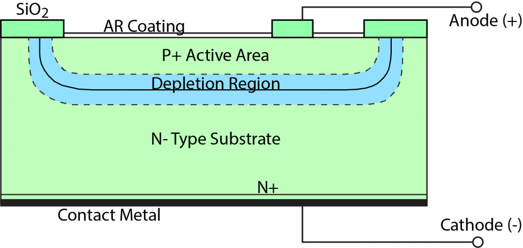
The depletion region creates a capacitance in the photodiode where the boundaries of the region act as the plates of a parallel plate capacitor. Capacitance is inversely proportional to the width of the depletion region. Reverse bias voltage also influences the capacitance of the region.
Key Performance Specifications
There are four major parameters used in choosing the right photodiode and whether or not to reverse bias the photodiode.
- Response (speed/time) of the photodiode is determined by the capacitance of the P-N junction. It is the time needed for charge carriers to cross the P-N junction. This is directly affected by the width of the depletion region.
- Responsivity is the ratio of photocurrent generated from incident light, to that incident light power. This is usually expressed in units of A/W (current over power). A typical responsivity curve of a photodiode will show A/W as a function of wavelength. This is called Quantum Efficiency.
- Dark current is the current in the photodiode when there is no incident light. This can be one of the main sources of noise in the photodiode system. Photocurrent from background radiation can also be included in this measurement. Photodiodes are usually put into
an enclosure that does not allow any light to hit the photodiode to measure the dark current. Because the current generated by the photodiode can be very small, dark current levels can obscure the current produced by incident light at low light levels. Dark current increases with temperature. Without biasing, the dark current can be very low. The ideal photodiode would have no dark current. - Breakdown Voltage is the largest reverse voltage that can be applied to the photodiode before there is an exponential increase in leakage current or dark current. Photodiodes should be operated below this maximum applied reverse bias or damage to the photodiode may occur. Breakdown voltage decreases with an increase in temperature.
Other important parameters include material, size of the photodiode and active area, and cost. Careful consideration is needed when browsing for photodiodes for your research or application. Photodiodes made from different materials (silicon, germanium, indium gallium arsenide phosphide, or indium gallium arsenide) have varying levels of sensitivity as well as differing speeds and dark current. Silicon, for example, provides sensitivity for wavelengths between ~400 and 1000 nm. However, it has the highest sensitivity at higher wavelengths (~900 nm). Germanium, on the other hand, provides sensitivity for wavelengths between ~800 to 1600 nm (with the peak ~1400 nm). The material of the photodiode is critical when finding the right photodiode to incorporate into your laser diode system.
Types of Photodiodes
P-N JUNCTION
This is the most basic photodiode. The physics of how the P-N junction photodiode operates was reviewed earlier. The PIN and APD photodiode are variations from the P-N junction.
The depletion region contains few free charge carriers, and the width of the depletion region can be manipulated by adding voltage bias.
Current passing through the photodiode can only flow in one direction based on the P and N doped materials. If reverse biased, current will not flow through a photodiode without incident light creating photocurrent.
PIN PHOTODIODE
The PIN photodiode is similar to the P-N Junction with one major difference. Instead of placing the P and N layers together to create a depletion region, an intrinsic layer is placed between the two doped layers. This layer is shown in Figure 2. This intrinsic layer is highly resistive and increases the electric field strength in the photodiode. There are many benefits to the added intrinsic layer because the depletion region is greatly increased.
The capacitance of the junction is decreased, and so the speed of the photodiode increased. The increased layer also allows for a larger volume of photon to electron-hole conversion and higher Quantum Efficiency.
Figure 2. PIN Photodiode Cross-section
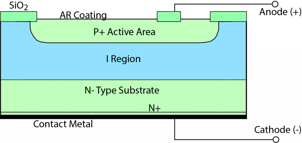
PIN photodiodes also have high frequency response. The major advantage of the PIN photodiode, compared to the P-N junction, is the high response speed from the increased depletion region.
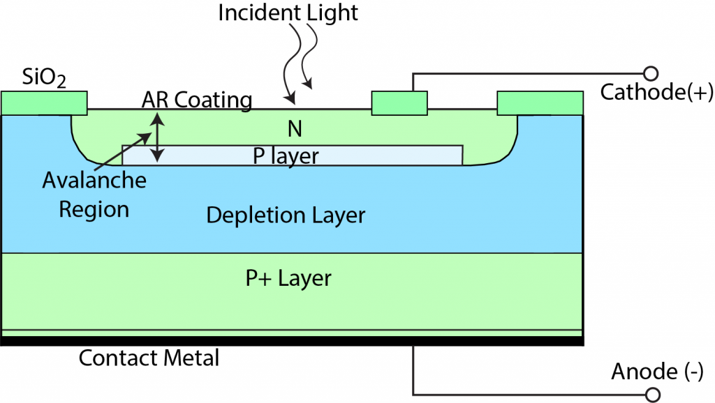
AVALANCHE PHOTODIODE
Avalanche photodiodes (APD) use impact ionization (avalanche effect) to create an internal gain in the material. APDs require high reverse bias operation (near reverse breakdown voltage). Each photo-generated carrier creates more pairs and so is multiplied by avalanche breakdown. This creates internal gain within the photodiode, which in turn increases the effective responsivity (larger current
generated per photon). Figure 3 shows the cross section of the APD.
The typical spectral response range is around 300 – 1100 nm. Current noise in an APD is higher than in a PIN photodiode, but the increased signal gain is much greater making signalto-noise ratio greater in APDs. APDs generally have a higher response speed and the ability to detect or measure light in lower levels.
Figure 3. APD Cross-section
Modes of Operation
“PHOTOVOLTAIC” MODE UNBIASED
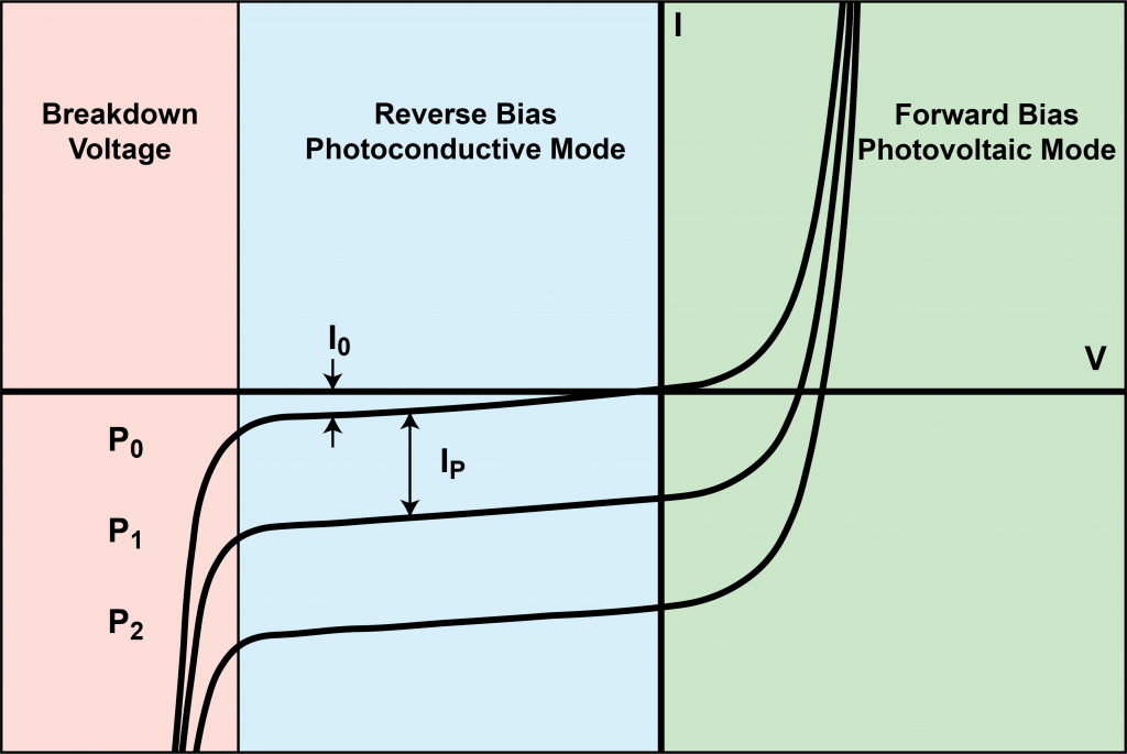
 Photodiodes can be operated without any voltage bias. APDs are designed to be reversed biased, so this section will be relevant to the P-N and PIN photodiodes. Without added voltage across the junction, dark current can be extremely low (near zero). This reduces the overall noise current of the system. Thus unbiased P-N or PIN photodiodes are better suited for low light level applications compared to operation with reverse voltage bias. (The reverse biased APD will still provide a higher sensitivity than P-N or PIN photodiodes for low light applications.) Unbiased photodiodes can also work well for low frequency applications (up to 350 kHz). Unbiased mode (where V = 0) can be seen in Figure 4 in between the forward bias mode (in green) and the reverse bias mode (in blue). The plot shows very little, if any, dark current when unbiased, which can be seen by the lack of current at the intersection of the I-V curve at V=0.
When the photodiode is illuminated, the electric field in the depletion region increases. This produces the photocurrent which increases with increasing photon flux. This is most commonly seen in solar cells where the generated voltage is measured between the two terminals.
Compared to biased mode, photovoltaic mode has less variation of photocurrent responsivity with temperature.
The major downfall with unbiased photodiodes is the slow response speed. Without bias to the system, the capacitance of the photodiode is at a maximum, leading to a slower speed.
“PHOTOCONDUCTIVE” MODE REVERSE BIASED
 When the photodiode is reverse biased, an external voltage is applied to the P-N junction. The negative terminal is connected to the positive P layer, and the positive terminal is connected to the negative N layer. This causes the free electrons in the N layer to pull toward the positive terminal, and the holes in the P layer to pull toward the negative terminal. When the external voltage is applied to the photodiode, the free electrons start at the negative terminal and immediately fill the holes in the P layer with electrons. This creates negative ions in the atoms with extra electrons. The charged atoms then oppose the flow of free electrons to the P layer. Similarly, holes go about the same process to create positive ions but in the opposite direction. When reverse biased, current will only flow through the photodiode with incident light creating photocurrent.
The reverse bias causes the potential across the depletion region to increase and the width of the depletion region to increase. This is ideal for creating a large area to absorb the maximum amount of photons.
The response time is reduced by the reverse bias by increasing the size of the depletion layer. This increased width reduces the junction capacity and increases the drift velocity of the carriers in the photodiode. The transit time of the carriers is reduced, improving the response time.
Unfortunately, increasing the bias current increases the dark current as well. This noise can be a problem for very sensitive systems using P-N or PIN photodiodes. This hinders the performance in low light situations. If using APDs, the signal to noise ratio will be large regardless because of the gain of the photodiode. Because a photon is ideally absorbed in the depletion region, the P layer can be constructed to be extremely thin. This can be balanced with the reverse bias to create an optimal photodiode with a faster response time while maintaining as low as noise as possible.
Another benefit to reverse biased operation is the linear output (straight line in blue section of Figure 4) of the photodiode with respect to the illumination. This simply means that the voltage and current change linearly (directly proportional) with increasing optical power. The non-linearity of the forward bias section (in green) can also be seen.
Figure 4 shows the reverse bias section (in blue) with the breakdown voltage next to it (in red). Photodiodes should not be operated beyond the breakdown voltage. This will damage the photodiode.
Figure 4. I-V Curve of Photodiodes. I0 is Dark Current. IP is photocurrent. P shows current at different light levels (P0 is no incident light).
Integration with Laser Diode
A monitor photodiode is often integrated into a laser diode package by the laser diode manufacturer. It produces a current partially proportional to the output laser diode optical power. If photodiode current is used as feedback, a control system will try to keep the photodiode current (and therefore the laser diode optical power) constant. The output of the adjustable current source will vary to keep the optical power level the same (this is called Constant Power (CP) Mode). Photodiode current and laser diode output power are related by a transfer function given in the laser diode datasheet.
Not only can photodiodes monitor the DC or CW output of a laser by providing current back to the laser system, they can also test a laser pulse shape and record peak powers of a laser pulse.
The information in datasheets for photodiodes include the four major components discussed earlier, the type of photodiode, peak sensitivity wavelengths, and most importantly size and cost.
Photodiodes that are already incorporated into the laser diode system can be limited in options and information. Laser datasheets usually give the maximum reverse voltage and sometimes the sensitivity of the photodiode.
If the specifications of the photodiode are extremely important to your laser design, custom builds or assemblies may be required to meet your needs.
Summary
When deciding to reverse bias your photodiode, or not, it all comes down to balancing speed and noise and deciding what is most important. If your application depends on extremely low noise and low dark current, you should choose to not bias your photodiode. If speed is your main concern, you should choose to reverse bias your photodiode as the response time is improved. In other words, if your
application is precision based, photovoltaic mode will better fit your needs. If your application is speed (high) based, photoconductive mode or reversed biased mode will better fit this area.
Reverse biasing the photodiode will be much more responsive than unbiased mode. If operating in photovoltaic mode, the response may need to be amplified.
The type of photodiode may also affect your decision of bias. Certain types of photodiodes can only be reversed biased, and others may have amplification of the response internal to the system. APDs will be effective in low light situations where sensitivity is critical but are expensive, P-N photodiodes are the most basic design and not widely used, and PIN photodiodes are the most common photodiode and the cheapest while having very low noise. As discussed earlier, the materials, size, and cost also affect the type of photodiode needed for the application. Table 1 shows a simplified chart comparing three different photodiodes.
Table 1. Comparison Chart
| P-N | PIN | APD | |
|---|---|---|---|
| PHOTOVOLTAIC | Best | Good | Poor |
| REVERSE BIASED | Good | Best | Good |
| LOW LIGHT | Poor | Good | Best |
| COST | Best | Good | Poor |
| LOW NOISE | Good | Best | Poor |
